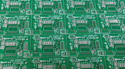
Compact-sized electronic devices have driven the demand for high density printed circuit boards or HDI PCBs. As the name suggests, these are the PCBs where components are densely packed on bare boards in multiple layers. These compact-sized packages assure excellent functionality and reduce sizes, too. Accomplishing this smallest functional package is not easy and demands expertise, experience, and the right use of technology. Like any other regular PCB manufacturing and assembly process, HDI PCBs also commences with design and layout. Owing to the complexities involved, this design and layout is an intricate process and certain things need to be addressed in this phase. This post gives tips for efficient PCB manufacturing and more.

Design Tips for HDI PCB
There are several things that you need to keep in mind when designing a HDI PCB. The following pointers will help you understand it better.
- Focus on the Right Design for Manufacturing (DFM): Design for Manufacturing (DFM) enables you to manufacture a PCB efficiently and cost effectively. In this phase, you need to focus on the right size, use of components, number of layers, and other technical details. Anything done in excess, may not only increase your manufacturing costs but also pose high risk of failure and lengthened manufacturing deadlines.
- Replace Regular Vias with Microvias: Microvias are the small holes or vias in the size equal to 150 microns. They are usually drilled on the bare boards using laser equipment. These vias are used to interconnect layers in the HDI PCBs. Drilling through-hole vias, buried, or bling vias is not easy on high density boards due to the different CTEs of copper and substrate. However, the laser equipment have small openings, so, they do not pose any problems with these different CTEs. To achieve it, you need to move the commonly used layers that have no traces or components on them to the top of the stack up. This would help you eliminate all other vias and replace them with microvias.
- Avoid Close Spacing or Crowding of Components: It is a misconception that HDI PCBs must have closely spaced components. The components must be placed symmetrically across vias, else there are chances that boards may warp or bend in high power applications. Also, the components may introduce high electromagnetic interference in traces, which may affect the signal quality. The improper placement causes uneven stress, which also heats up the components triggering their early failure.
- Choose the Right Stackup to Reduce Material Costs: The selection of the right stackup is important for the efficient performance of PCBs. This is because the number of layers or materials impact drilling cycles and lamination costs. The following are a few common types of HDI stackups:
- 1+N+1: This stackup comprises 1 build-up of high-density interconnection layers
- i+bN+i (i≥2): This stackup may have two build-up of high-density interconnection layers
- i+N+i (i≥2): They feature buried vias
- Focus on Signal Integrity Factors: Signal integrity is one of the key factors that determines the success of HDI PCBs. Using shorter trace widths is recommended to achieve brilliant signal integrity. In addition to this, one also needs to focus on factors like analog and power signal isolation, adequate planes in ground, consistent path impedances, and so on.
As the functioning of electronic devices depends on these PCBs, it is important that you get them designed and manufactured from trusted manufacturers. There are many manufacturers who offer these PCBs in custom specifications to meet your application requirements. Twisted Traces is one such experienced manufacturer that specializes in custom HDI PCBs. The company has been delivering these PCBs to its clients for use in commercial, industrial, and mission-critical applications. Everything right from quote to manufacturing to after-service support is handled by industry experts at the company.
It was the same with the question of his cottage. buy cialis But why not telephone.


