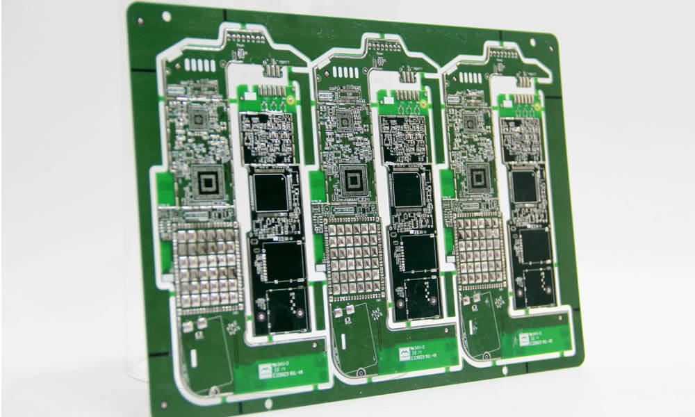
Pcb circuit board wiring, that is, laying the road of the power signal to connect various devices, is like connecting various cities to traffic by road repair. In pcb circuit board design, wiring is an important step to complete product design. It is also the step with the finest skills and the highest limit. Even experienced engineers have a headache for wiring.

The following are important rules for PCB layout. As long as you are engaged in PCB board related work, you should master:
1.Direction control rules
The input and output wires should be avoided as much as possible. When the Pcb circuit board is routed, the routing directions of adjacent layers are orthogonal structures, avoiding different signal lines in the same direction in adjacent layers, so as to reduce unnecessary interlayer interference. When the Pcb circuit board wiring is limited by the structure (such as some backplanes), it is difficult to avoid parallel wiring, especially when the signal rate is high, you should consider using a ground plane to isolate each wiring layer and a ground wire to isolate each signal line. The schematic diagram of the routing direction of the adjacent layers is shown below.
2. Open-loop inspection rules
In order to avoid the "antenna effect" caused by wiring and reduce unnecessary interference radiation when wiring the Pcb circuit board, it is generally not allowed to have a floating form at one end, otherwise it may bring unpredictable results.
3. Length control rules
That is, the short-line rule. When designing, you should try to keep the wiring length as short as possible to reduce the interference caused by too long traces, especially some important signal lines, such as clock lines. Be sure to place its oscillator close to the device. The place. In the case of driving multiple devices, the network topology should be decided according to the specific situation.
4. Impedance matching check rules
The wiring width of the same network should be kept the same. The change of the line width will cause the uneven characteristic impedance of the line. When the transmission speed is high, reflection will occur. This situation should be avoided as much as possible in the design. Under certain conditions, such as connector lead-out wires and BGA-packaged lead-out wires, similar structure may not be able to avoid the change in line width, and the effective length of the inconsistent part in the middle should be minimized as much as possible.
5.Chamfering rules
When the PCB board is routed, a bend in the trace is inevitable. When a right-angle corner appears in the trace, additional parasitic capacitance and parasitic inductance are generated at the corner. The corners of the routing curve should be avoided to be designed in acute and right angle forms to avoid unnecessary radiation. At the same time, the technical performance of the acute and right angle forms is not good. It is required that the angle between all lines and lines should be greater than or equal to 135 °. In the case that the wiring does need right-angle corners, two improvement methods can be adopted: one is to turn the 90 ° corner into two 45 ° corners; the other is to use rounded corners, and the rounded corner method is the best. ° Corner can be used at 10GHz. For 45 ° corner traces, the corner length should preferably satisfy L≥3W.
6. Device decoupling rules
A. Add necessary decoupling capacitors to the printed board to filter out interference signals on the power supply and stabilize the power supply signal. In multi-layer boards, the location of decoupling capacitors is generally not too high, but for double-layer boards, the layout of decoupling capacitors and the wiring method of the power supply will directly affect the stability of the entire system, and sometimes even the design Success or failure.
B. In the double-layer board design, the current should generally be filtered by the filter capacitor before being used by the device.
C. In the design of high-speed circuits, whether the decoupling capacitors can be correctly used is related to the stability of the entire board.
7, 3W rule
In order to reduce crosstalk between lines, it is necessary to ensure that the line spacing is sufficiently large. When the center distance of the lines is not less than 3 times the line width, 70% of the electric field can be kept from interfering with each other, which is called the 3W rule. If 98% of the electric field does not interfere with each other, a pitch of 10W can be used.
8.Ground circuit rules
The minimum loop rule is that the loop area formed by the signal line and its loop must be as small as possible. The smaller the loop area, the less external radiation and the smaller the interference from the outside.
9.Shield protection
Corresponding to the ground circuit rules, it is actually to minimize the loop area of the signal. It is more common in some important signals, such as clock signals and synchronization signals. For some particularly important and high-frequency signals, copper shaft cables should be considered. The design of the shield structure is to use isolated ground wires to isolate the laid lines, and how to effectively combine the shielded ground with the actual ground plane.
10.Resonance rules
Mainly for high-frequency signal design, that is, the length of the wiring must not be an integer multiple of its wavelength to avoid resonance.


